Design of a well performing Phase Locked Loop (PLL) system is not for the
faint hearted!. In this article I am setting down the results of my reading
on the subject.
Any engineers out there who find errors feel free to correct me. Bear in
mind that I have not yet got a loop to work as I would like.
In a single loop system there are tradeoffs between step resolution,
lockup time and sideband noise A problem area is stability of the loop
which is not well covered In most articles on the subject. For example a
Motorola app note suggests you "check loop stabilty using Bode plots" but
does not give any further details.
I have built a synthesizer using a setup in another manufacturers' app note
and found it to be unstable, especially when modulated.
As I am not professionally trained I find the theory of analysis of PLLs
rather daunting.
However there are a number of programs around which will analyse the PLLs
for stability and other parameters. In particular, the software written by
KD9JQ is available freeware and gives useful info on a loop setup.
A Phase locked loop can be represented as(Fig 1)
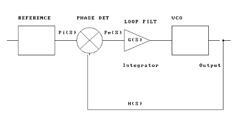
Fig 1`
Pi(s) represents the phase of the reference oscillator, while Pe(S) is the
error phase signal which is filtered and used to drive a VCO. The transfer
function of this section is represented by G(S).
H(S) represents the feedback transfer function to the phase detector. An
equivalent more practical system is shown in Fig 2.
A Voltage Controlled Oscillator (VCO) can be swept over th frequency range
of interest by a control voltage. The output of the VCO is the output of
the PLL system which is used as the Local Oscillator of a receiver for
example. Some of the VCO output is fed back and compared with a reference
frequency in a Phase Detector (PD) The reference is usually a crystal
oscillator but might be the output of another loop for example. The PD
generates an error volatge which steers the VCO to lock it to the same
frequency as the reference. This simple system produces an output on the
same frequency as the reference crystal oscillator. In a practical system
it is necessary to add a programmable divider, a reference divider and a
loop filter
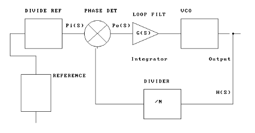 Fig2
Fig2
In a typical practical system, the VCO operates at a frequency in the VHF
or UHF region while the reference is typically in the HF region (say 4
MHz).A typical frequency step might be 25 KHz (eg in the 2M FM segment). In
this case the PLL reference divider will divide the crystal reference by
160 (4MHz -> 25 KHz). For a VCO output on (for example) 146.5 MHz the main
divider would be set at 5860 to divide 146.5 MHz down to 25 KHz. Thus when
the loop is locked, the reference and VCO signals presented to the phase
detector are both 25 KHz. The final component in the system is the loop
filter. This is necessary because a typical phase detector does not
generate a "DC" error voltage but rather a pulsed waveform depending on
the loop lock situation. For example the Motorola MC145170 PD output is a
logic level signal with positive or negative going pulses. (depending on
how the chip is programmed). If this waveform were applied directly to the
VCO a broad, frequency modulated signal would result. The loop filter
integrates (or averages)the PD output to produce a smooth error voltage.
VCO design
There is much debate about VCO design which is considered somewhat of a
"black art"! However a few principles can be stated.
The oscillator should use good quality components in a circuit which will
produce a reasonably stable low noise signal even before the PLL is
connected. I have found the grounded gate FET circuit works but no doubt
there are other opinions on the optimum circuit. The circuit inductor
should be as high a Q as possible. Some designs have even used a section of
solid coax as a transmission line inductor. In 52 MHz and 144 MHz designs I
have elected to use an S18 series inductor from Cirkit in the UK.(Fig 3)
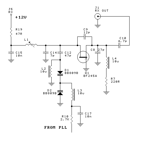
In this circuit the values were for a 52 MHz oscillator.
Most VCOs are tuned with a voltage variable capacitance diode (varicap).
The diode is reverse biased with the VCO control voltage. These are
relatively low Q devices and will tend to degrade oscillator noise
performance. Thus they should have minimum coupling to the tuned circuit -
just enough to achieve an adequate frequency swing. Ideally the full tuning
voltage range of the diode should be utilized. (normally 0.5-30V). The
tuning voltage should not be zero or the diode may be forward biased during
part of the oscillator cycle and degrade performance.
The supply for the VCO should be regulated and decoupled and the oscillator
should probably be shielded. A suitable buffer circuit should isolate the
VCO from any load.
The VCO gain is important in designing the loop filter. This figure is a
measure of the frequency swing of the VCO per unit change in the VCO
control voltage. For example, a VCO which changed frequency from 144-148
MHz with a control voltage swing of 0.5 to 8.5 V would have a VCO gain of
0.5 MHz/Volt.
Phase Detector
The phase detector is normally integrated into the PLL chip along with
programmable reference and main divders and digital control circuitry.
There are several possible phase detector circuits.
For example, e 74 series EX OR gate can be configured as a phase detector.
Most modern PLL chips use a charge pump circuit. The output of this is a
logic level pulsed waveform which is integrated to produce the VCO control
signal. An important parameter in designing the loop filter is the Phase
Detector Gain which may not be easily available from the manufacturers data
sheet.
This is a measure of the change in output voltage of the Phase Detector
with a change in the frequency/phase difference between the VCO and
reference frequencies. PD gain is expressed in Volts/Hz or Volts/Radian (1
Hz = 2*pi Radians)
Loop Filter
As stated above, the loop filter integrates the pulsed output from the
phase detector to produce a smoothed "DC" VCO control voltage. The loop
performance can be set by varying the component values in the loop filter.
Various loop filter configurations are possible. (Fig 4)
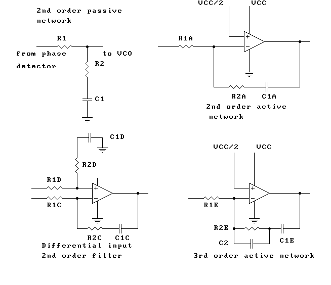
The simplest is an RC low pass section. This will always include a second
resistor in series with the capacitor to "damp" the response. An
un/underdamped loop will "ring" after a frequency step, ie swing back and
forth for some time before final stable lock is achieved. This is simplest
"second order" loop which is adequate for many applications. A further
section of RC filtering can be added to produce a third order loop with
improved sideband and noise performance. (C2 in the opamp circuit).
However it is more difficult to analyse higher order loops for stability
and other parameters.
If a simple RC filter is used, the VCO control voltage swing is limited to
0-5V in systems with a digital phase detector. For best phase noise
performance it is necessary to use the full available control range of the
varicap diode. To do this, a second opamp can be configured as a DC
amplifier to bring the output voltage to a higher figure (say 30V) (Fig 4).
All components in the loop filter should be designed for low noise (eg low
noise opamp and metal film resistors). In the example above of the 144-148
MHz VCO, 1mV of noise will produce a 500 Hz swing of the VCO ouput fequency.
Programmable divider
The dividers are incorporated in the PLL chip in modern designs. The
MC145170 has a 16 bit main divider with a "legal" divide range of 40 to
65535. The input to the divider is buffered to accept AC coupled voltages
from the VCO/buffer up to 160 MHz. Earlier designs (eg MC145152) used an
external dual modulus prescaler to divide the VCO output down to less than
20 MHz. A dual modulus prescaler has two divide ratios under the control of
the main PLL (eg divide by 10/11).
By switching between the two ratios partway through the divide cycle, the
PLL has much finer frequency step resolution. This is best understood by
looking at the maths.
PLL control
Most modern designs use a serial interface from a microcontroller to load
data to the synthesizer.
A serial interface is difficult implement using EPROMs or TTL logic. This
makes it difficult fot hobbyists without access to a micro and suitable
programming skills to use these chips.
See my Programmable PLL board for VHF for a user
programmable system without the need for writing code!
In the case of the MC145170, a 3 wire interface is used (DATA, CLOCK and
ENABLE). A 24 bit serial word will update both main and reference
registers. An 8 bit word will update the control register which sets such
things as phase detector polarity, lock detect output and clock setup.
Phase noise
A critical parameter in PLL design is phase noise performance. Phase noise
is in effect frequency modulation of the VCO output by noise.
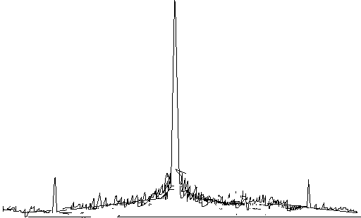
Fig 5
Poor phase noise performance will degrade the overall system noise
performance in a receiver for example. Noise sidebands may mix with strong
adjacent signals to reduce receiver dynamic range. In a transmitter phase
noise will show as noise adjacent to the carrier which may interfere
with other services. The PLL will reduce noise outside the loop filter
bandwidth. Thus a low filter cutoff frequency improves phase sidebands at
the cost of slower lockup time. Inside the loop filter bandwidth noise is
determined by the VCO noise and noise added by the loop. VCO noise can be
minimized by a low noise transistor, run at optimum current and high Q
components in the tuned circuit. PLL noise can be minmized by low noise
components in the loop filter and good quality supply voltage. The
reference to the loop will also contribute noise but in practice this is
not a problem where the reference is a crystal oscillator, as a crystal has
very good phase noise performance.
Other spurious outputs
Any spurii on the reference will be reproduced in the output of the PLL.
This may be problem where the reference is the output of another loop or a
Direct Digital Synthesizer (DDS), for example. The amplitude of these spurs
will increased by a factor proportional to thb frequency multiplication
involved. The other main spurious output is related to the reference
itself. In the case of the 25 KHz reference example (above) sidebands will
appear 25 KHz above and below the main carrier. They will be attenuated by
the loop filter, depending on its bandwidth.
Ideally the reference frequency should be at least 50 times the filter
cutoff.
Some terms
Various terms such as "second order"," third order" and "phase margin" are
used when describing PLL design. The "order" of the loop relates to the
mathematical equations used to desribe the transfer function of the loop.
A second order loop has only one RC section in the loop
filter/integrator. In practice, a true second order loop does not exist as
there will always be additional RC sections introduced by the loop
amplifier open loop pole and circuit stray capacitance etc. A third
order loop has an additional RC pole which improves sideband
attenuation but makes analysis of the loop more complex. Some references
use a second order loop with an additional pole at approx 10 times the 2nd
order loop cutoff frequency. They assume the additional pole will not
significantly alter the phase/stability response and use a second order
calculation as an approximation to loop behaviour. Damping factor
(which describes the behaviour of the loop to a transient or step in
frequency) can be calculated for a second order loop but not
for a third. Phase margin is used to desribe loop stability in a
third order loop. (fig 6)
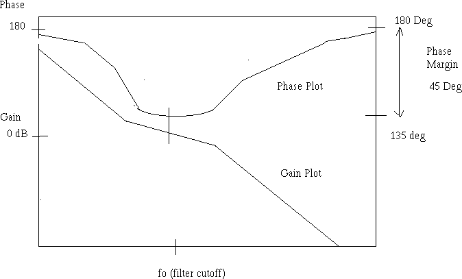
Fig 6
(Forgive the crude drawing!) Figure 6 shows the open loop gain/phase
response of the loop. If at filter cutoff fo loop gain is 1 ( 0 dB) or
greater and phase is too close to 0 (or 180 in the case of a PLL) then the
loop will be unstable and oscillate. The difference between 180 and the
actual phase response at the phase "inflection" (ie minimum) is known as
phase margin. Ideally it should be in the range of 30-70 degrees (45
optimum). Higher phase margin will result in a more stable loop but less
sideband suppression.
Loop Design Sequence
Assume a synthesizer is to be designed for a 6 metre FM rig with a frequency
range of 50-54 MHz. Step size will be 25 KHz over the whole band. The
Motorola MC145170 will cover this frequency range with minimal external
components.
Available VCO supply voltage is 12V to give a VCO control range of say 1 to
11V. VCO gain Kv is thus
(54-50)/10 = 0.4 MHz/volt or 400000 Hz/volt.
Assume that the loop bandwidth should be a maximum of 1/50 of the reference
frequency to allow acceptable sidebend suppression. Maximum loop bandwidth
is therefore
(25000/50) = 500Hz
Note that lockup time is inversely proportional to loop bandwidth - ie
higher loop bandwidth gives a quicker lockup time. Note that a higher loop
bandwidth will mean less reference sideband suppression and but better
close in VCO phase noise suppression. For an amateur receiver, loop lockup
time is not critical and anything less than 10-20 msec would be acceptable.
We will thus aim for a loop Fo (loop filter cutoff - approx equal to 3 dB
bandwidth) of about 100Hz.
Kp or phase detector gain is VDD/4pi for the single ended output and VDD/2Pi
for the differential output of the MC145170.
For a 5V supply (VDD) Kp is 0.398 or approx 0.4 for the single ended and 0.8
for the differential output. I have elected to use a 2nd order filter circuit
with an additional opamp for DC gain. This allows a wider VCO control
voltage range and eases the design of the loop
The circuit of the PLL is shown in
Fig 7.
I have cheated on the loop calculations and used the freeware program from
KD9JQ


to calculate the
loop components for a 2nd order PLL with the following parameters:
Freq range 50-54 MHz
Freq step 25000 Hz
Loop Type 1 (active)
Bandwidth 100 Hz
Damping factor 0.7
VCO Gain (Kv) 400000 Hz/V
PD gain(Kp) 0.8 (differential output)
Phase det type 6 (tristate FF)
DC Gain (Ka) 2.6
Division (N) 2080 (midband figure)
Opamp open loop gain 100000
Ref freq 25000 Hz
The initial value of R2(damping resistor) was entered as 2200 Ohms
and the other values adjusted to 12 K and 2.2 uF as in the circuit
With these values and the above figures, the following results
were obtained:
Bandwidth 103 Hz
Locktime 3.2 msec
Reference suppression -50.7 dB
VCO noise suppression -27.7 dB
Damping factor 0.75
I have built this circuit for a 6 meter transceiver project. Using a
spectrum analyser to observe loop behaviour it appears to be stable
and behave predictably. I have not formally measured phase noise performance
but it looks OK on the spectrum analyser!