The following assumes that you have read the AD9852 data sheet from first to last page...
I have breadboarded an AD9852AST, which is the variant that can be clocked to 200 MHz. The 300 MHz version, the AD9852ASQ, has a 'thermal slug' on the bottom of the chip. This slug can be thermally coupled to a (well ventilated) cooling block to dispose of the heat dissipated in the chip.
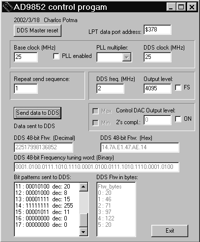
I have written a small program in Borland's Delphi to control the AD9852 from the parallel port of a PC. This program allows for the entry of the clock frequency, the calculation of DDS output frequency and subsequent programming of the AD9852. It is also possible to activate the built-in PLL clock-multiplier to achieve higher clock speeds with a moderate speed chrystal clock module. A word of warning here: watch out for overheating the chip! The program allows for a 300 MHz clock speed, but you are responsible for monitoring the chip temperature. It is entirely possible to destroy an uncooled chip in a matter of seconds!
The control program is focused on the display of the calculated 48-bit frequency tuning word in various formats. Read the program source to get an idea of how this tuning word is calculated. Apart from the frequency tuning word, all bytes sent to the AD9852 are shown in a list.
The program also allows for setting the DDS cosine DAC output level using a 12-bit (0-4095) word. The second DAC output level may also be specified in a 12-bit 2's-complement format. The output of this DAC is a DC voltage. It could be used to generate the X-voltage when the AD9852 is used in sweeper application.
The program initialises the AD9852 after a Master Reset to activate only the digital section and the cosine DAC. The sync filter is not activated as this filter is very power hungry. The AD9852 can be reset at any time with the 'DDS Master Reset' button. After each change of one of the input fields the 'Send data to DDS' button has to be pressed to actually send the chip setup and calculated frequency tuning word to the AD9852.
After a Master Reset, the chip defaults to the internal update mode, meaning that at regular intervals the input data is sent from the input buffer registers to the digital circuitry. This can be monitored by measuring the update pulses on pin 20 (I/O UD) which is configured as an output after a Master Reset. Although internal update may be useful (one pin less to wire), I have chosen to initialise the chip to use external update mode so that the actual update moment is determined by the controlling program. After setting the chip to external update mode, the pulses on pin 20 dissapear and this pin is set to be an input. The AD9852 may be damaged if this pin is directly connected to any external source that is at ground level during the time between a Master Reset and setting the chip to external update mode. This is because the 3 Volt output pulses are then shorted to ground and the digital output current rating for this pin may be exceeded. A simple 1k resistor sets this current to a safe maximum of 3 mA.
The schematic shows the interface circuit between the 5 V PC parallel port and the 3.3 V AD9852. This interface is taken from the schematic of a similar project by OH8RO . The 10k resistors pull up the lines to 3.3 V, while the schottky diodes isolate the 5 V from the parallel port from the AD9852 3.3 V. The schottky diodes also set the 'zero level' of the input lines to approximately 0.3 Volt.
I have used an LM3940 as a 3.3 V low-drop regulator. The schematic shows only one regulator, in a practical application at least three are needed: one for the clock module an one each for the AD9852 analog and digital power supply. These regulators should be well isolated from each other to improve the SFDR.
The AD9852 is programmed using the serial data mode. This is set by grounding pin 70 (S/P SELECT).
This means that pins 1-8 (D7-D0: the bidirectional parallel programming data inputs) are not used
and are grounded. The pins 17, 19 and 20 (IO RESET, SDIO and I/O UD) are used to clock the data
bits into the chip. These pins share their function with port A (Parallel Address Inputs). Pin 18
(SDO) is not used and left unconnected. Pins 14, 15 and 16 (A5, A4 and A3) are not used and are grounded.
Pin 21 (SCLK) acts as data clock and pin 22 (CSB) as chip select.
I used a 25 MHz clock module. Other frequencies may of course be used. The clock frequency is a parameter in the control program, so it can be changed at will. The chip is set to asymmetric clock input by grounding pin 64 (DIFF CLK) and pin 68 (REFCLKB) and feeding the output of the clock module directly to pin 69 (REFCLK). Most clock modules designed for 5 V will run on 3.3 V as well. If not, additional interface circuitry is needed.
The AD9852 is breadboarded on a small piece of PCB where the copper layer is used as a ground plane. All pins not connected to ground are bent up a little bit. All ground pins are soldered directly to the ground plane. All power pins are decoupled with a SMD 100nF capacitor directly from pin to ground. The remaining pins are wired with thin enamel wire to contact strips of veroboard, allowing for easy modification of chip configuration. The DAC outputs have an unfiltered 50 ohm termination. The schematic is basically following the AD9852 data sheet.
Control program with Delphi source
Send your comments (email address is on my home-page)