I have been playing with an AD9854, which is a complete direct digital synthesis circuit in a 80 pin package. It needs only a reference clock and some filtering to make a very practical frequency source from DC to low VHF.
The older DDS IC AD9850 from Analog Devices Inc has been used for local oscillators in radio receivers and transmitters. For controlling it a microcontroller with an optical encoder and an LCD module has been used. AD9854 should be better than the former one, because it has 12b DAC (10b in AD9850). The manufacturer ADI specifies 10 dB better narrowband spurious levels ( 6 dB wideband ) for the AD9854. It also has other features such as quadrature outputs and digital modulation capability.
It came to my mind that some other people might like to use the software I wrote while testing the circuit. The program is useful for either initial testing - to see that the circuit is working all right - or even as a means of setting and tuning AD9854 as a receiver LO or a simple signal generator.
Controlling AD9854
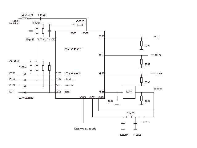
An easy way to hook up the controlling circuit is in serial mode from PC's parallel port. Some interface circuitry is needed, because AD9854 is specified for 3.3 V supply voltage.
Fig. 1 shows, how the interface is made. It is not very fast, but either side can be hot or cold without blowing anything on the other side. Voltage drop over schottky diodes is 0.2 V.
For serially controlling AD9854 at least data and clock lines are needed. For the IC to accept the data the chip select line must be down. The program sets it down for each loading even though it could be down all the time, as no other device is sharing the data and clock lines. Chip select can be used as a trigger signal to look programming pulses with a scope.
A pulse to the IOreset line is needed if something goes wrong with loading. The program sends IOreset pulse with every load sequence for certainty. The device needs a positive master reset pulse after DC power is switched on. It is not provided by the program.
The program
With the program AD9854C.exe one can set and tune the frequency in CW-mode. For use as a receiver LO also IF can be given and the both possible receiving frequencies are printed on the screen. The level in Q-outputs can be varied by giving the wanted attenuation in dB. This function is done by controlling a 12b digital multiplier in the device. In this case the level decreases somewhat with increasing frequency as it does in DDS devices. Alternatively the inverse sinc correction can be chosen, in which case the output is flat and high.
Look the help in AD9854C.exe (F1) for more details. The program runs under DOS with VGA. The LPT address can be given in the program. The program is free for personal and amateur use.
Features
The following is only some remarks. For more information get the available data from ADI.
The analog outputs are -80...-10 dBm. An amplifier stage is needed to drive a standard level diode mixer as an RX LO. One I-output is used to drive the comparator to get a rectancular signal, and that is why I-outputs are kept high all the time.
The comparator is able to drive a 50 ohm load with +10 dBm.
The power dissipation of the device depends heavily on the clock frequency and the features used. With a 100 MHz clock it draws 340 / 260 mA depending if the inverse sinc filters are in use or not.
Due to a 48-bit wide frequency tuning word the resolution is extremely fine, less than 1 uHz. Near the output frequency the spectral purity is very good comparing to LC oscillators, but wideband spuriouses can be down only about 60 dB. Because of the way in which the frequency is generated, very high components occur also at the clock frequency +/- the wanted baseband frequency. An LP filter is needed to filter out these components. In practice the upper limit for the output frequency is about 35 % of the clock frequency. If the clock frequency is 100 MHz, and we program the DDS to give out 35 MHz, there exists a strong frequency component at 100 MHz - 35 MHz = 65 MHz, which must be suppressed in the LP filter. If the wanted frequency is increased, the spurious gets closer, and becomes more and more difficult to suppress.
The reference clock
It is possible to clock an AD9854 up to 300 MHz, but that with using the thermally enhanced ASQ package with proper pc-board design to get the heat out of the device. Using a cheaper AST package the maximum clock rate is 200 MHz. It is possible to use lower clock frequency by activating PLL in the device, which multiplies the clock frequency. However, the output spectrum is cleaner (especially nearby) when the PLL is disabled as is case when using the AD9854C.exe.
Notes on the circuit and assembly
The clock is fed to the differential clock inputs terminated by a 680 ohm resistor matched to 50 ohm of the master clock oscillator output. Level can be -10...-3 dBm. The circuit stops working at -30 dBm.
A fabricated pc-board is not absolutely necessary, but it would ease things a lot. I used 0.8 mm 2-sided copper glad board material just as a ground plane. It is divided into digital and analog grounds by splitting the upper folie so that the border runs under the IC near pins 30 and 68. Several SMB connectors fix the board mechanically to a 2 mm thick aluminium plate making also rigid electrical connections. This plate is the cover of a milled metal box housing the circuitry.
A 15 pin D-connector is used for control and DC connections.
Most pins of the 80 pin package are either GND or NC and can be readily soldered to the ground plane. Hot pins were carefully bent up. To each group of power supply pins a 15nF 0805 capacitor was soldered and 3.3 V supply was connected via a 2.2 ohm series resistor to avoid parallel resonances in the shunt capacitor net. Over 3.3V there is yet a 220nF chip of 1210 size quite near the IC. I have used a common supply for the analog and digital sections during the initial tests, but for high performance separate supplies or some LC-filtering on the analog side may be needed.
To enhance heat transfer some silicon heat sink compound was put under the IC.
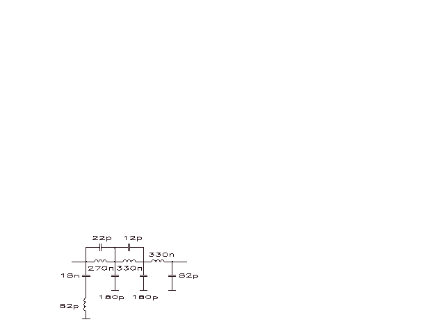
Low-Pass filters
Figure 2 shows one possible low-pass filter for 0...30 MHz. Two units were made using 1206 components and the performance was very similar. For best results the filter sections should be shielded by metall walls. Attenuation from 67 MHz upwards is nearly 90 dB if shielding is good. I also used thin 1 mm coax in connections between AD9854 and the LP to the comparator. That LP was constructed on a separate pc-board to be easily replaced if needed. The other LP was constructed in a separate metal box to be coupled to one of the outputs outside the main DDS box.
Ideas and applications
- RX LO
- In AD9854 there are two I- and two Q-outputs. Each pair is in opposite phase and between I- and Q-outputs there is 90 deg. phase difference, which remains 90 deg. whatever the frequency. This makes possible to simplify many balanced mixer designs and image cancelling mixer designs.
- Using the same AD9854 for both RX and TX
- Frequency switching is very fast. Psk and amplitude modulation features are worth a look.
- A phasing type SSB generator
- The needed quadrature RF signals are available. The whole HF range needs no bandswitching or mixing.
- AF signal generator
- Would need only an instrument amplifier and some reed relays to have a larger output level range with PC control. Often the available 100...200 mV rms to 50 ohms is adequate with no amplifier stage needed.
- FSK/ PSK test generator, CW test generator, sweep generator
- Frequencies can be set with great accuracy. Can be keyed by a digital signal.
- A very clean and stable RF signal generator by phase locking a low noise LC oscillator to AD9854.
- A new life to that old SMDU, perhaps, excellence in near signal measurements.
It is worth noting, that once the basic DDS circuitry and its control are at hands, the rest of the circuitry for an application is often quite simple.
Just to record
All the information is believed to be accurate ... and so on...
However, don't blame me for blowing your circuits. No quaranties given. No responsibilities taken. None, whatsoever.