Frequency Counter/VFO Stabilizer
Richard Hosking VK6BRO
Software VFO Connections
Construction Troubleshooting
Boards and controllers are
available from the author
Introduction
Most new receivers and transmitters use synthesized local oscillators which are
locked to a crystal standard. However there are still many older or new
homebrew rigs with free running local oscillators which are prone to drift.
Often they do not have a frequency readout which is virtually mandatory in
today’s crowded bands. This article describes a board which can be used to
stabilize a free running local oscillator and provide a frequency readout in
one package.
Functional description
The board consists of a front end gate/prescaler circuit, a microcontroller and
a loop filter/VCO control circuit using a passive integrator and voltage
follower.
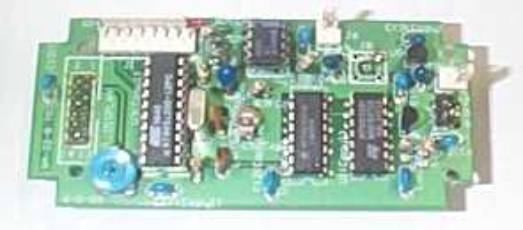
Fig 2 Top
view of completed module
The front end samples the VFO signal, squares it up, gates and prescales it
under the control of the microcontroller. The microcontroller counts the frequency
of the VFO, decodes the data and displays it on an LCD display module. The
controller itself has only an 8 bit counter which contains the most significant
8 bits of the count data at the end of each count period (100 msec). The
prescaler U2 (74HC 4020) contains the other 14 bits of data. To access this the
prescaler is toggled via U1:C (pin 9) until the prescaler output changes state.
The controller keeps track of how many pulses are required and from this
calculates the contents of the prescaler. Thus the overall resolution is 22
bits. This means that frequencies up to about 40 MHz can be counted to a
resolution of 10 Hz which should be adequate for most applications. The
controller converts the binary data to BCD and ASCII to drive the LCD display.
PLL circuit
The controller compares the frequency from one count to the next. If the loop
is locked, the controller corrects any drift in the VFO by outputting a
positive or negative pulse to an integrator/filter circuit. This is buffered by
a voltage follower so that there is no significant voltage sag across the
filter capacitor between counts. The voltage follower output is connected to a
varactor diode which must be placed across the VFO tank circuit. The varactor
should produce a frequency swing of about 5 KHz for a control voltage swing
between 0.5 and 4.5V. If the VFO is likely to drift more than this then it
should probably be redesigned or repaired!
If the error between counts is more than 50 Hz it is assumed the VFO is being
tuned and the loop is unlocked. In this case the circuit sets the VCO control
to midrange and waits until there are 3 counts without change before locking
the loop again. There is no need to manually lock the loop and the PLL system
is invisible to the user.
Offsets
Most rigs use an IF and many also have a mixing scheme to allow use on several
bands. Also with SSB rigs there are usually different BFO frequencies for USB
and LSB. Thus the readout from the VFO will require a method of setting offsets
to give the actual operating frequency. In this case the board has 4 I/O lines
available to select offset frequencies. Thus there are 16 possible offsets
which can each be individually set by the user to 10 Hz resolution with
positive or negative offset. Note that it is only necessary to ground the I/O
pin as there are on board pullups on these inputs. (Fig 3)
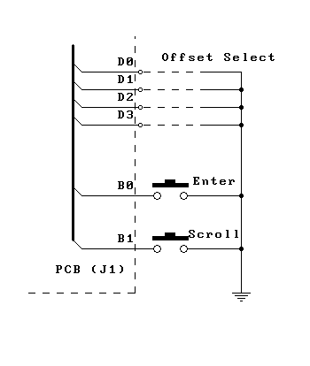
Fig 3 Offset select connections
The data, once entered, is stored
in the controller nonvolatile EEPROM memory. To enter the offset data the user
connects two pushbutton switches between bits 0 and 1 of port B and ground. If
ENTER (bit 0) is grounded during normal counter operation then the controller
enters the offset setup code routine. The user is prompted to enter
"POS" or "NEG" for offset. The SCROLL (bit 1) key is used
to select the appropriate option. When ENTER is pressed again, the program
moves to the offset frequency. The flashing cursor indicates which digit is
being entered. The SCROLL key advances the digit from 0 to 9 and then rolls
over to 0 again if SCROLL is pressed repeatedly. When ENTER is pressed, the
next digit is selected. Note that the final digit is always 0 to indicate the
frequency in Hz. After the final digit is entered the program returns to normal
counting. The Offset data is stored in the EEPROM at an address selected by the
4 offset select lines. The user should set these lines appropriately before
entering the setup program. When the counter is in operation it accesses the
EEPROM at the address selected by the offset select lines and adds/subtracts
the offset from the VFO frequency accordingly.
Controller
The controller is an Atmel AVR device AT90S1200. This controller has a program
memory of 512 bytes, EEPROM and serial "flash" programming. This
means that the controller can be placed in position in the circuit where it is
to used and programmed in-situ if desired. The program memory appears quite
small but due to the rich instruction set quite compact code can be written. In
fact this program took nearly all of the available memory (510 of 512 bytes!)
PLL analysis
As far as the PLL is concerned, the controller is merely an intelligent phase detector.
Assuming that the VFO can be shifted 5 KHz by the PLL with a swing of 0.5-4.5
V, then the VCO gain Kv is 5000/4 ie 1250 Hz/V. The frequency count takes about
120msec with a pulse duration to the sample and hold circuit of 2 msec per 10Hz
error. Thus phase detector gain Kp is 4*(2/120)/10 V/Hz or 7.5 mV/Hz. Using the
PLL analysis program from KD9JQ with the loop values as shown (RC 82K and 33uF,
damping 2.2K) then the 3dB loop bandwidth is 9.8 Hz and lock time is 34msec.
The 10 Hz "reference" (ie the correction pulse) is not significantly
attenuated and is audible on the VFO output, but in practice this was not a
problem. If the 2.2K damping resistor (R10) is omitted, the attenuation of
correction pulses is improved. In this case the resistor is replaced by a short
circuit. In theory this would result in an unstable loop but as the loop does
not have to capture lock, it does not appear to be a problem in practice.
Display
The board has been designed to interface with 16 character by 2 line displays
with a 4 bit parallel interface. This interface appears to be a defacto
industry standard for these small displays. Initialization is rather involved.
See the LCD article for more detail on initialising
and driving these displays
Some displays (eg Sharp) should mount directly via 0.1 inch spacing connectors (eg IDC style). Alternatively a cable can be made up using an IDC socket/plug or wiring the connections individually. If the backlight is to be used it will require about 2.3V at 70-100mA.
Display connections are as follows:
PIN
1 GND
2 VCC (+5V)
3 Contrast
4 R/S (Register select - data/command)
5 R/W (Read/Write -grounded to write)
6 OE (Enable)
7-10 NC
11 Data4 (Bit 4 data)
12 Data5
13 Data6
14 Data7
15 NC
16 Backlight
17 Backlight
Software
The count sequence is described in “pseudocode”
Reset
prescaler
Open
gate/start count
Wait
100msec
End
count
Toggle
prescaler until the output changes state (keep track of number of toggles)
Calculate
22 bit binary count
Convert
count to BCD
Add/subtract
offset from EEPROM
Write
to display
PLL
routine
Repeat
sequence
The PLL routine is shown below
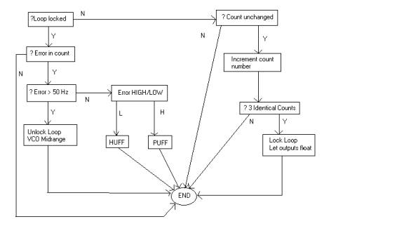
For those who are interested to improve or modify the code I have
included full source in assembler. I would be interested in any comments.
Source code for the counter/stabilizer
Definitions for the stabilizer
VFO
Connections
Connections to the VFO/rig will depend on the rig circuit. A typical scheme is
shown in Fig 4.
In valve rigs beware of high voltages! If voltages are more
than 50V then use high voltage blocking capacitors at the input to the counter
(C4) and for C1 in Fig 4.
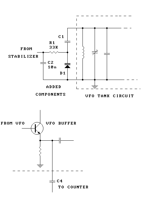
Fig 4 VFO connections
If the board is to be built
into an existing rig then it will be necessary to make connections to the VFO
tank, the VFO output and an 8-12V supply. Consult the rig circuit diagram to determine
the appropriate connections. The components D1, R1 and C1 should be added
across the VFO tank circuit. Use the smallest value of C1 possible consistent
with obtaining a sufficient tuning range (5 KHz). This will have to be
determined by experiment. As an example the author used this circuit to
stabilize a 5-6 MHz VFO. In this case the varactor used was a BB405B VHF diode
with C1 2pf. Bear in mind that a varactor is a low Q device which may add to
VFO noise or even cause the VFO to stop oscillating. If the varactor loads the
VFO too much the tuning range could be reduced to 3 KHz without too much
problem. The VFO will almost certainly have a buffer circuit. A sample should
be taken at the output of the buffer via C4 for the input of the counter. (in
this case I have shown an emitter follower buffer but of course each rig will
have a different configuration) The counter input presents an impedance of
approx 1000 ohms so the takeoff point should be reasonably low impedance. The
counter requires approx 100 mV Pk-Pk for satisfactory operation.
Construction
The counter is built on a double sided, plated through, masked and overlaid
PCB. Fig 5 shows a top overlay. Mount the polarized components carefully
(diodes/ICs/tantalums). Build the regulator section first and check that the
supply is +5V before proceeding further. It is probably a good idea to use a
socket for the controller though this is not mandatory. Be careful with static
sensitive devices (ICs/controller) by keeping them in conductive foam before
mounting and not handling with ungrounded objects. If the display is to be
soldered in place it is a good idea to wire the display via a temporary harness
to check operation of the counter before permanently wiring the display. (Note
that the underside of the board will be inaccessible for troubleshooting once
the display is mounted). As the board is quite simple it should not present any
great difficulty to a constructor of intermediate experience.
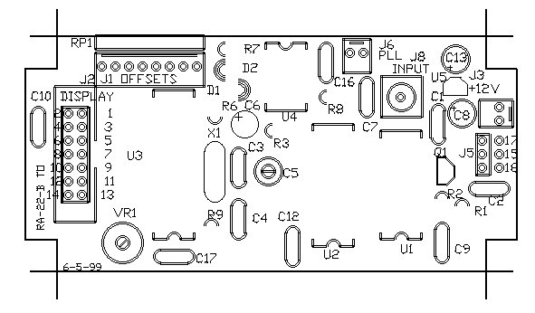
Fig
5 Board Overlay
Troubleshooting
Usually there will be at least one error in the construction of a project.
Before powering up the board check your construction again (avoid the
temptation of skipping this bit!) Check the polarity of each component and go
over the board with a magnifying glass to check for bad joints and shorts.
Check for shorts to ground from +5V. Check that there is continuity between +5V
and the relevant pins on each IC. If the board does not work first time adopt a
systematic approach to troubleshooting. Assuming the regulator works correctly,
first check the front end circuit by applying a signal of approx 200 mV PK-PK
and look the output of the squarer (U1 pin 6). A square wave at the input
frequency should be present. Check pins 4 and 5 of the controller where a 4 MHz
clock signal should be present. Check the connections between the board and LCD
module for continuity. There should be a series of pulses at a repetition rate
of about 10 Hz on the control lines to the prescaler and the LCD data lines.
Adjust VR1 to give best display contrast. If you are still in trouble check
every single connection on the board for continuity and this should find the problem.
Assuming the counter is working correctly, set the clock to exactly 4 MHz.
Apply a signal of known accuracy to the counter and adjust C5 until the correct
reading is obtained.
Component List
Resistors (axial 1/4 W)
1K2 2 R2,R8
2K2 1 R10
4K7 1 R11
10K 1 R9
82K 2 R6,R7
100K 1 R1
10K Trimpot 1 VR1
10K Resistor X 7
commoned SIL pack 1 RP1
Capacitors (ceramic unless specified)
10n 1 C1
1u Tant 2 C8,C13
1u 1 C7
10p 1 C3
22p 1 C4
33u Electro 1 C6
40p Ceramic trimmer 1 C5
100n 7 C2,C9,C10,C11,C12,C15,C16
Misc
4MHz Crystal low profile 1 X1
(HC9/U base)
1N4148 diodes 2 D1,D2
74HC00 1 U1
74HC4020 1 U2
78L05 1 U5
AT90S1200 1 U3(Programmed- available from the author)
2N3904 1 Q1
DISPLAY 1 16 character by 2 line LCD display
(eg Hitachi HD44780, Powertip 1602)
TL081 1 U4
SMB PCB mount socket 1 J8
0.1" pitch PCB headers 2 pin 2 J3,J6
0.1" pitch PCB header 8 pin 1 J1
PCB 1 (Available from the author)
0.1" pitch pin header or IDC 14 pin socket and plug/ribbon cable
to connect to displayKD9JQ
Homepage Software for
PLL analysis and homebrew page
Eamon Skelton EI9GQ Great homebrew projects
Frequency counter
module from which I copied the idea!
Disclaimer
Each homebrewer should check that modifications to his rig are safe and that
the desired result will be achieved. The author accepts no responsibility for
damage to equipment or persons as a result of using this circuit. Check with
someone who has the relevant knowledge if you are not sure.!
Buy a board and controller